
Glass PCB

you can read about PCB basics from here
The following figure shows the stages of the process of obtaining fees using photoresist:

1. Covering the material with foil .
2. Apply photoresist
3. Exposure
4. Manifestation
5. Etching
6. Remove photoresist
As a blank, the master takes a glass plate, without sharp edges, and :
2. Apply photoresist
3. Exposure
4. Manifestation
5. Etching
6. Remove photoresist
As a blank, the master takes a glass plate, without sharp edges, and :

To which copper foil will be applied (thickness is 0.05 mm is optimal):

With the help of superglue:

And this is a film photoresist:
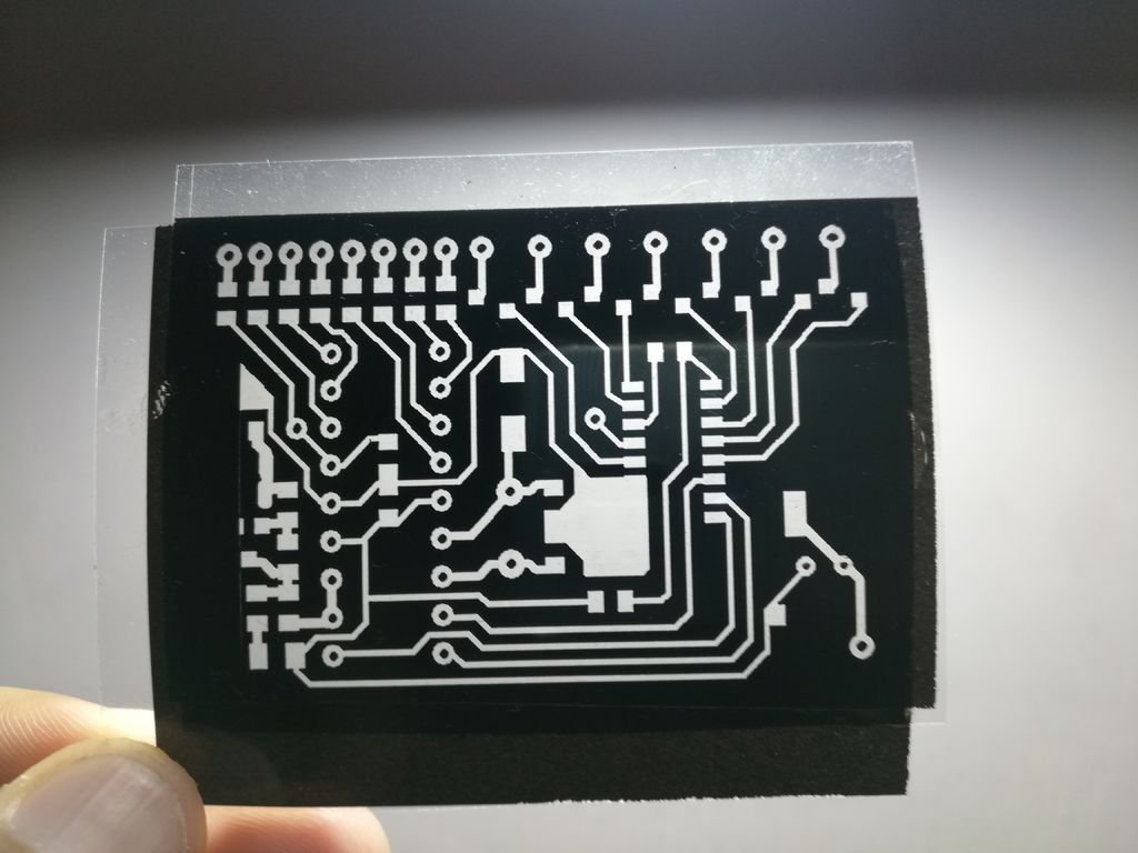
The hdissanayake scheme is in EasyEDA:

In the same program, he designs and PCB:

The drawing of which displays in a negative form, since this type of photoresist becomes insoluble under the action of ultraviolet:

Prints on film:

In this photo, both the foil and the glass are already degreased with isopropyl alcohol:

And here - already glued to each other with the help of superglue, which is important to apply evenly, without air bubbles and uncovered areas, squeeze out excess glue, wait for full setting:
Master removes the photoresist from the substrate:

And sticks on copper, again avoiding bubbles:

Imposes a printout on the film, presses the glass, presses the clips so that they do not obstruct the ultraviolet:

It exposes with bright sunlight for 5-7 minutes, after removing the printout, the illuminated photoresist looks like this:

Scotch removes the second substrate on the opposite side of the photoresist:

Places soda solution to develop:

Washes off the solution along with the unlit photoresist:

Alternates the development and washing, until the non-illuminated areas of the photoresist is completely washed off:

Fee charges ferric chloride as usual:

Almost ready, it seems, ferric chlori


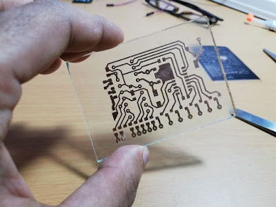
It remains to wash the lighted photoresist - if the water is hot, he will succumb. And the art of glass printed circuit boards can be considered revived. The board is ready for soldering. As shown in the photo, do not hold glass without gloves:

In this card, for obvious reasons, there can be no holes. But this is not so uncomfortable. Because there were no holes in the board in the same B3-04. And now, when there are SMD components for all occasions, it is even easier.
Comments: 0
Post a Comment